
We Analyzed 495 AMD Radeon and Nvidia GPU Specifications and Shared the Dataset with Everyone
About the Dataset
In Datalore we’ve manually assembled a dataset with the technical specifications of 495 Nvidia and AMD Radeon GPU machines. Let’s learn more about how this type of hardware has improved over time.
How to open the notebook in Datalore?
Datalore is an online Jupyter notebook with smart coding assistance hosted by JetBrains. Datalore comes with an intelligent code editor and powerful computation machines.
Click the “Edit” button in the upper right corner in this notebook.
Dataset overview
The dataset contains details of 495 GPU models:
- GPU manufacturer.
- GPU class.
- Name.
- Year of release.
- Fab = fabrication process (nm).
This defines the size of the transistors in the processor. - Number of transistors (millions).
- Die size
- Memory size in megabytes.
- GFLOPS = billions of Floating Operations Per Second (32-bit precision).
- TDP (thermal design power) = the maximum amount of heat generated by a computer chip or component.
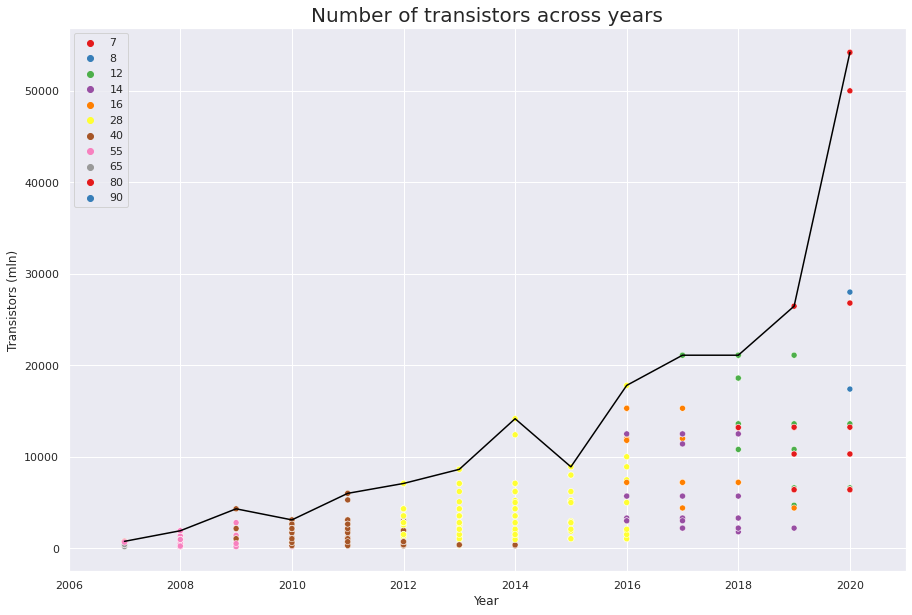
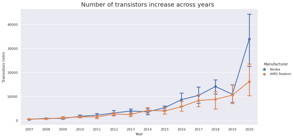
Moore’s law for transistors
Moore’s law says that the number of transistors in an integrated circuit doubles every 2 years. Let’s see whether it applies to GPUs as well!
As we can see from the plot below, Moore’s law holds true for 2019-2020, but in 2006-2018 growth was almost linear.
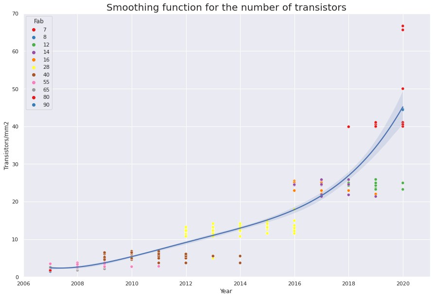
However, Moore’s law is almost true for transistor density. If you look at the plot below you’ll see that it doubles roughly every 3 years.
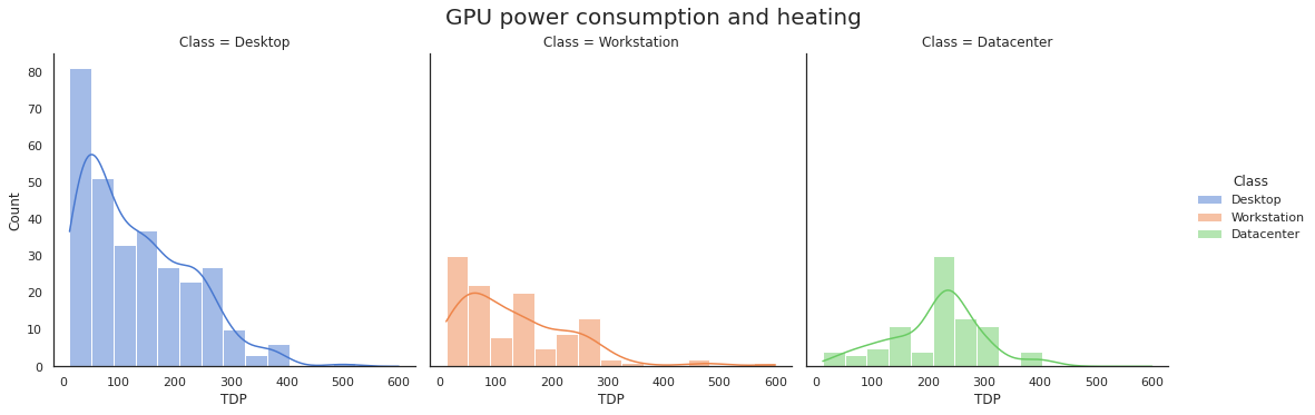
GPU power consumption and heating
Another interesting topic is GPU power consumption and heating.
This dataset splits GPUs into three groups:
- Consumer GPUs, e.g. Nvidia GeForce and AMD Radeon R series.
- Workstation GPUs such as Nvidia Quadro and AMD Radeon FirePro.
- Server GPUs, e.g. Nvidia P/V/T series and AMD Radeon Instinct.
Let’s display the distribution of TDP (thermal design power) for the 3 GPU groups. We’ll plot the exact distribution in bins and add a smoothed line approximation.
💡 Insight:
While server GPUs are hotter and more powerful on average than consumer and workstation ones, it’s interesting that there are a lot of low-power workstation GPUs. These are intended not for 3D graphics or parallel computing, but for managing display panels and video walls.
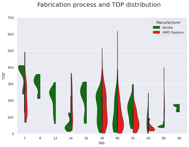
Fabrication process and TDP distribution
In the next plot we see how the GPU model distribution changes depending on the fabrication process and the TDP across two manufacturers.
💡 Insights:
- There is no clear correlation between manufacturer and chip TDP, nor is there a clear correlation between fabrication process and TDP.
- Although the power consumption of transistors decreases as they become smaller, the growing number of transistors on a chip outweighs this effect.
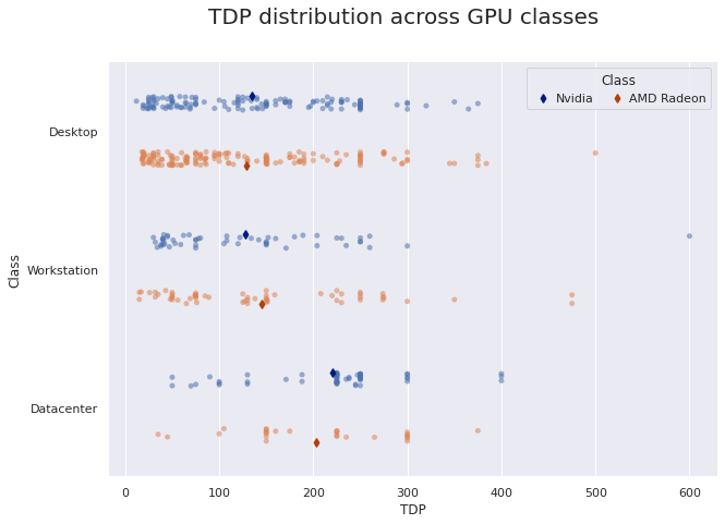
TDP distribution across GPU classes
Let’s display the TDP distribution across classes and manufacturers, ignoring fabrication process level.
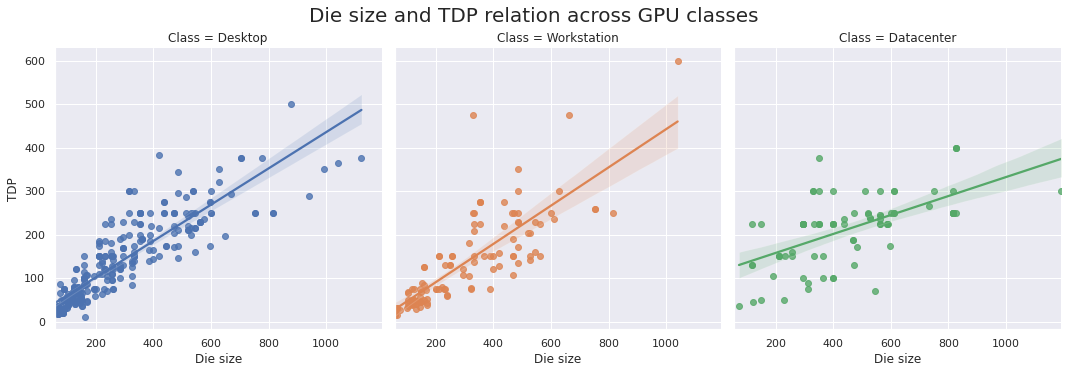
Die size and TDP relation across GPU classes
From the plots below we can see a linear correlation between TDP and the physical amount of silicon, including die size.
GFLOPS progress
GFLOPS is the number of billions of Floating Operations Per Second. It determines the computational power of a GPU. Let’s see how this number has increased over the years.
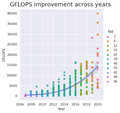
We’ll also compute an additional feature – the number of GFLOPS per million transistors:
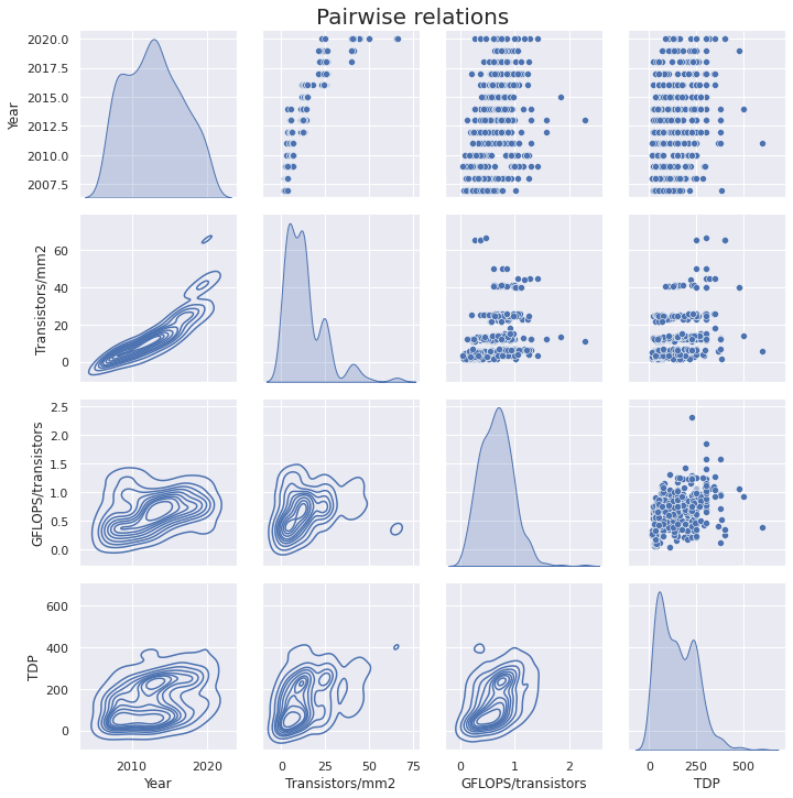
Pairwise relationships
On the plot below we can see the dependencies between the year, transistors/mm2, GFLOPS/transistors, and TDP parameters.
💡 Insights:
- The spike around 250 W TDP is caused by the prevalence of this value among both AMD and Nvidia’s top-tier chips. However, Nvidia RTX 30 GPUs are much hotter than their predecessors: the RTX 3080 and 3090 are rated at 320 W and 350 W TDP, respectively, and the AMD RX 6800 XT is 320 W.
- While Nvidia chips are generally larger than AMDs, in 2020 the gap between the sizes of their chips is bigger than ever, as the new 54-billion transistor A100 chip has been released. The interesting thing though is that AMD has more or less the same GFLOPS and TDP across its smaller chips as its larger counterpart.
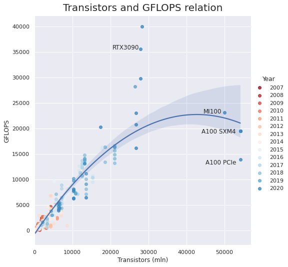
Transistors and GFLOPS relation
From the plot below we can see that the Nvidia A100 and Radeon MI100 have roughly the same FP32 GFLOPS as the other top-tier GPUs of 2020 and 2019, despite having ~2x many transistors. Still they are significantly slower than the desktop-segment RTX 3090, which has nearly twice as many GFLOPS.
However, A100 and MI100 have significantly faster FP32 sparse and FP16 modes. For example, while the RTX3090 yields only 35.6 TFLOPS of FP16, the MI100 can provide up to 184.6, and the A100 can reach 624 when working with structurally sparse matrices. It seems like this is caused by the new Multi-Instance GPU technology, which allows the A100 to be partitioned into seven GPU instances.
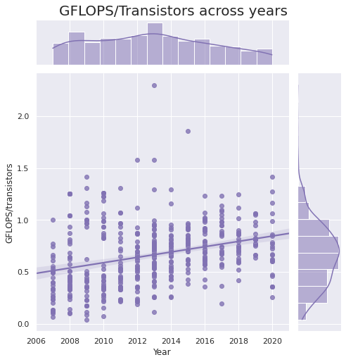
A final interesting observation is that there is almost no growth of GFLOPS per number of transistors.
💡 A final interesting observation is that there is
almost no growth of GFLOPS per number of transistors.
Check out the summary plots in Datalore!
Feel free to play with our GPU dataset, which is available here. Please mention the Datalore team as the source of the Dataset. We would love to see your work and share it with our community.
Subscribe to Datalore News and Updates


